The connection between UV light curing technology and 5G technologyread count [710] release time:2019-12-24 20:36:00
UV light curing Technology is currently blooming everywhere in the application field. In addition to the printing, silk screen, inkjet coding and other industries that we are often exposed to, can you imagine that UV light curing technology is actually related to 5G technology? What is the specific relationship? uv Let us take a look at how light curing technology supports 5G technology.
The insulation properties of materials are very important to the power and electronics industry. For high-voltage power equipment, the insulation of insulation components or support materials directly affects the safety and stability of power transmission. The development of 5G technology is in full swing today. For 5G, a high-frequency communication technology, low Dk/Df materials are one of the keys. Dk is the dielectric constant of the material, and Df is the loss factor. These factors are directly related to the insulation performance of the material itself, especially the insulation performance under high-frequency working conditions. There are many ways to make low Dk/Df materials, including epoxy sheets using SMA as a curing agent, cyanate ester materials, and fluorine-containing materials.
Fluorinating the material surface to improve the insulation of the material is a good method to improve the insulation of the material. Commonly used material surface fluorination treatments include direct fluorination treatment and corona-assisted fluorination treatment. However, both methods have the disadvantages of toxic working environment and short effective time. Both methods are also limited by the lack of integrated manufacturing technology, thus affecting their promotion in industrial applications.
The working group of Professor Zhang Guanjun of the State Key Laboratory of Electrical Insulation for Electrical Equipment, School of Electrical Engineering, Xi'an Jiaotong University, used photocuring method to modify the material surface with fluorine, and achieved good results.
The method used by Professor Zhang Guanjun is to add the fluorinated methacrylate monomer DFHMA (molecular formula as shown in Figure 1(b)) to the photosensitive resin (High Temp, a commercial product from Formlabs), mix it thoroughly, pour it into the mold, and cover it with a PET film. A heating unit is applied to the back of the mold, and then the material is cured using UV LED (wavelength 405nm). The amount of fluorinated monomer added shall not exceed 5% (w/w).
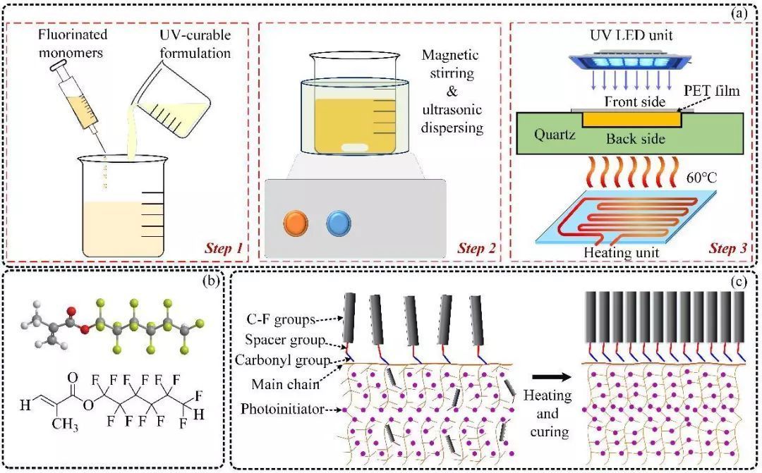 Figure 1 (a) Workflow for material modification, (b) chemical structure of fluorinated methacrylate monomer DFHMA, and (c) surface aggregation effect of fluoride
Materials with added fluorinated monomers, although the addition amount is relatively low (no more than 5%), will accumulate in large quantities on the surface of the cured material due to the surface aggregation effect of the fluorinated monomers. Comparison with the blank sample without added fluorinated monomer shows that the water contact angle of the material can be increased from 65° to 92°.
The surface flashover and bulk breakdown strength tests of the material showed that the first flashover voltage (Ufb) did not increase significantly, but the condition voltage (Uco) increased from 21.8 to 26.4kV, and the delay voltage (Uho) also increased significantly (Figure 2(a)). The improvement in delay voltage (Uho) shows that the introduction of the fluorinated monomer DFHMA enables the material surface to obtain better resistance to degradation and leakage resistance. The bulk breakdown strength of the material is also significantly improved (Figure 2(b)).
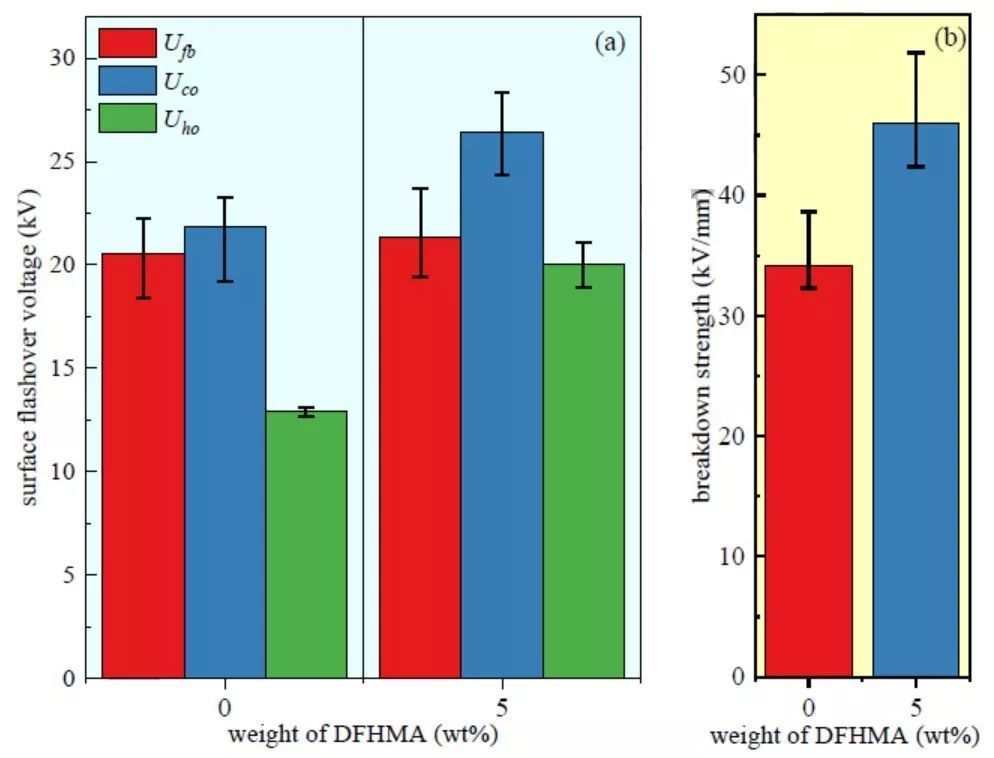 Figure 2 (a) Pulse flashover strength, (b) 50Hz bulk breakdown strength of different samples
This work by Professor Zhang Guanjun's working group shows that surface fluorine modification of materials using UV light curing technology can effectively change the surface properties of the material without changing the bulk properties of the material. This method has good prospects for the design and manufacture of insulating materials, and provides a simple and easy way to improve dielectric properties for the power and electronics industries.

The update and iteration of 3C electronic products is accelerating, and consumers have increasingly higher requirements for the appearance of products. In addition to beautiful colors and comfortable feel, the surface is also required to have excellent scratch resistance. It is also expected that the product surface has anti-fingerprint and anti-graffiti properties. The surface of the product is not easy to leave fingerprints and other traces during use, or even if traces are left, they can be easily erased.


